Technology
What Is PariPoser® Technology
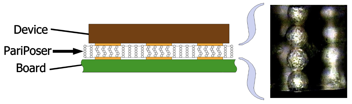
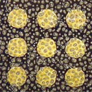
PariPoser® material is an anisotropic conductive elastomer. BallWire® columns conduct vertically, while an insulating silicone matrix provides electrical isolation laterally.
Why PariPoser®?
Key Technology Highlights
Thin & Fast
Low self-inductance, typically below 0.1nH, makes PariPoser® material ideal for high-speed interconnections, with electrical performance that approximates an underfilled solder joint far better than a spring pin.
Flexible
Since there are no pads that have to be aligned to the substrate, a single piece of PariPoser® material can simultaneously accommodate unique features such as waveguides right along conventional LGA pads.
Reliable
Unlike some heavily filled “elastomers” with a large fraction of metal, PariPoser® material is mostly silicone, and retains its resilience even after hundreds of thousands of cycles.
Cost Effective
Low cost per line makes our solutions ideal for test applications and high-volume production.
Explore More
PariPoser® History
The PariPoser® technology was developed at Bell Labs in the 1980s. Bell Labs anticipated the future needs of the electronic industry for higher speeds and increased densities, and knew that interconnects would play a big part in meeting those goals. When the lab was broken up in the 1990s, Paricon acquired the technology, the equipment, and the patents with the goal of commercializing the technology.
Benefits & Purpose
PariPoser® material is good for high-speed interconnects, because it is so thin. It’s good for power interconnects because it has a high Current Carrying Capacity (CCC). It’s good for high-durability applications because the material does not take a set. And, it’s good in wet environments because it is impervious to liquids.
How Does It Work?
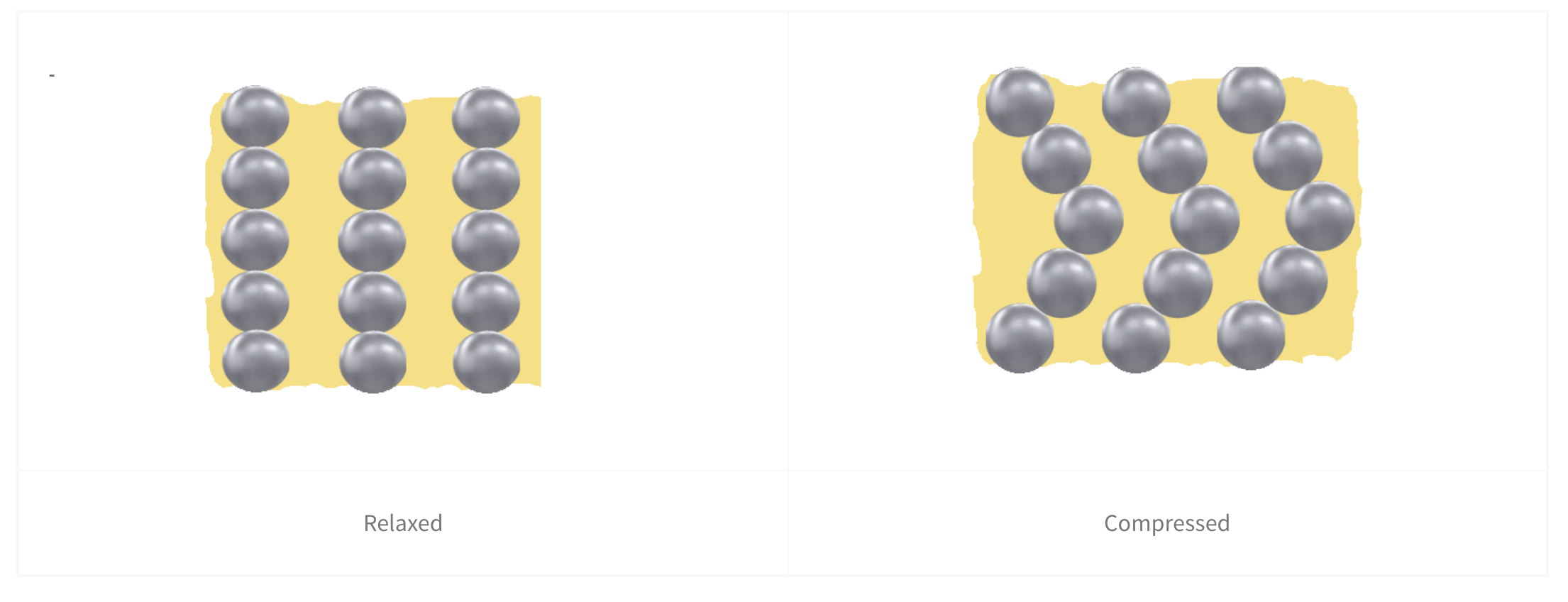
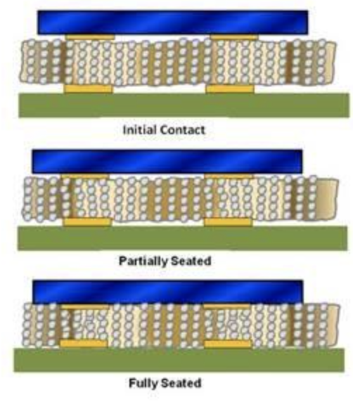
When the material is relaxed, the silver-plated particles at the end of the columns stick out a bit from the silicone. So, as soon as contact is made, these columns immediately conduct current. As the material is compressed (typically <30% of the thickness), the metal particles push against each other, and the CRES drops down to about 10-20 mΩ.
Silicone has an unusually low Young’s modulus in comparison to its bulk modulus. To facilitate compression at the pad locations, there needs to be some adjacent area into which the silicone can squeeze. Typically, that area is the space between the PCB or DUT pads – as shown in the illustration below. The expansion areas need to be uncluttered (no solder mask, no traces, and no components).
PariPoser® Material Versions
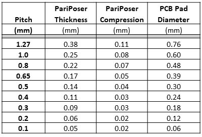
When the pitch of the contacts (and the size of the pads) gets bigger or smaller, there should still be 6-10 columns for each pad, so the spacing of the columns and the size of the particles must be adjusted for each pitch. (Small PCB pads need more closely spaced columns and thus smaller particles.) Each column has 4-5 particles, so when the diameters of the particles change, the overall thickness of the elastomer sheet will also change.
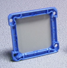
Stretch frames
PariPoser® material can be attached to a metal or plastic frame, keeping the material taut and making it easier to handle, with a higher temperature rating (up to 150°C). When not mounted on a stretch frame, the loose material’s temperature rating is 100°C.
When mounted taut on a stretch frame, the silicone is already a bit thinner than normal due to the stretch, and it takes more thermal expansion before the silicone fills in the interstitial spaces.
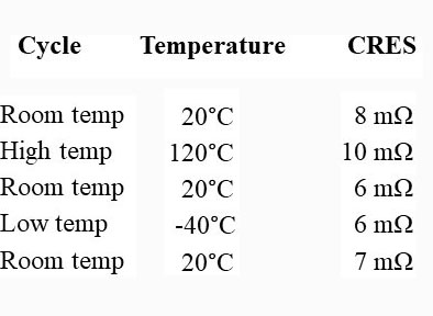
Thermal cycling within the specified limits of -50°C to +150°C will result in very little variation in CRES. Actual thermal cycle results for 1.0mm pitch material are shown below. The cycles were repeated many times with consistent results.
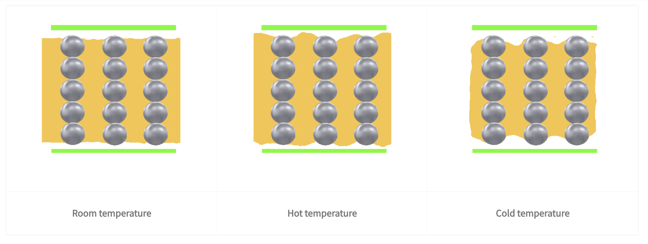
In addition to the vertical CTE effect, there might also be horizontal expansion and contraction. The CTE differences among the interconnection materials (PariPoser® material, the PCB, and the DUT) might result in horizontal misalignments.
CCC (Current Carrying Capacity)
PariPoser® material has multiple short columns of nickel particles per contact position. This results in a low resistance and low inductance path for the current compared to most connector geometries.
Markets
Markets for PariPoser® Technology
Test
Because PariPoser® material is about as thin as a solder joint, it’s electrical performance mimics an underfilled solder joint better than spring pins enabling much higher frequencies. High density PariPoser® connects copper pillars with diameters under 0.1mm.
OEM - Defense
High reliability and redundancy which are key attributes for defense applications.
Healthcare
Excellent signal integrity and repeatable performance that simplifies device assembly, improves testing accuracy, and support the miniaturization and durability demands of medical equipment.
AI/Datacenters
Supporting efficient assembly, maintenance, and scalability of high-performance networking and computer hardware.
Telecommunications
Connectorization makes systems repairable and upgradable.
Space
Passed NASA space reliability/outgassing specifications. More resilient than solder to resist thermal cycling.
Optical Transceivers
Ideal when devices cannot be soldered.
Custom Solutions
Liquid tight barrier for DNA sequencing.
Annular connections around wave guides can be built into an LGA.
Extreme high speed: Radar, Lidar, etc.
Our Technology At Work
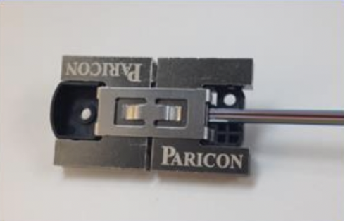
Connector for Optical Transmitter and Receiver
Bench Top and Handler Test Sockets
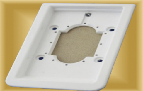
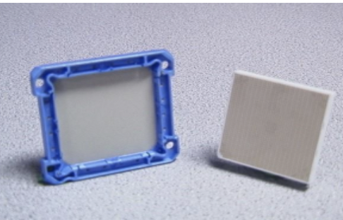
Frame with PariPoser®
Connect and protect DNA sequencer